Custom PCB design is crucial for modern electronics. Many devices now require IoT connectivity. This integration can be challenging for designers. One main issue is keeping the PCB design compact while ensuring connectivity. Moreover, engineers often struggle with component selection, signal integrity, and the layout of the board. Without proper planning, devices may face connectivity issues in the IoT ecosystem. Understanding how to navigate these problems can lead to better products and improved performance. 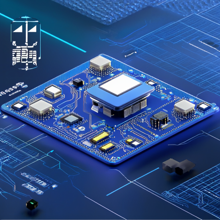
Integrating IoT connectivity in custom PCB design involves careful planning and consideration of various factors, including component selection, layout, and signal integrity.
Selecting the right components is essential. Choose parts specifically designed for IoT applications. These components often have low power consumption and small footprints.
The PCB design must accommodate various communication protocols. Wi-Fi, Bluetooth, and Zigbee are popular options. Ensure you understand their specifications and limitations.
Signal integrity can affect performance. Use proper routing techniques and ground planes to minimize noise. Simulation tools can help verify the design before manufacturing.
A compact layout reduces the size of the PCB. Use multi-layer designs and optimize component placement. This step helps in maintaining effective signal flow and reducing interference.
IoT devices often run on batteries. Implement power management techniques to extend battery life. Consider using low-power components and efficient voltage regulation.
Prototyping is necessary to validate your design. Use testing tools to evaluate the connectivity and functionality of your custom PCB. Iterating on design based on feedback will help refine the final product.
Devices like smart thermostats use custom PCBs designed for IoT connectivity. They integrate numerous sensors and communication protocols effectively.
Wearables require compact designs and low power consumption. Advanced PCB designs have revolutionized the industry, offering functional devices that fit in small spaces.
In conclusion, integrating IoT connectivity in custom PCB design is essential for modern electronic devices. By focusing on component selection, layout strategies, and testing methods, designers can create efficient PCBs. Understanding these factors can lead to better devices in the competitive market. Qingjian Electronics specializes in providing custom PCB designs that meet these requirements.
What is PCB design? PCB design involves creating layouts for printed circuit boards to connect electronic components.
Why is IoT connectivity important? IoT connectivity allows devices to communicate and operate within a network, enhancing functionality.
How does one start custom PCB design? Begin by understanding your project requirements, selecting components, and using design software to layout the PCB.
Copyright © Shenzhen Qingjian Electronic Technology Co., Ltd. All Rights Reserved | Sitemap
Recommend Products: Low Volume PCB Prototype Production Services Single Sided PCB Prototype Fabrication Services Quick Turn PCB Prototype Services PCB Prototype Lead Time Small Batch PCB Prototype Quotes Multilayer PCB Prototyping Services


